
Once relegated to the domain of niche applications and university research, Micro-Electromechanical Systems (MEMS) are now stepping confidently into the center of semiconductor innovation. The shift from lab experimentation to fab-level integration reflects not just a maturation of MEMS technologies but a fundamental reimagining of what chip design can encompass. Erik Hosler, a strategic thinker in semiconductor patterning and emerging lithography techniques, acknowledges that MEMS is no longer a side note but is becoming part of the script.
This development is unfolding across multiple fronts. As traditional Moore’s Law scaling becomes more difficult, engineers are looking for new ways to enhance functionality without relying solely on shrinking feature sizes. MEMS is answering that call by offering mechanical, optical, and electromechanical components that work alongside or within conventional silicon logic. The result is a richer, more multidimensional approach to chip architecture, one that incorporates sensing, motion, and adaptation directly at the silicon level.
A Short History of MEMS in the Semiconductor World
MEMS has existed as a concept for decades. The earliest devices, such as pressure sensors and accelerometers, were typically developed independently of digital logic and manufactured in specialized foundries. These devices served specific markets like automotive safety, industrial sensing, and biomedical monitoring.
While useful, MEMS development remained separate from mainstream semiconductor flows. Engineers working on logic and memory chips often had little contact with those designing mechanical sensors. Toolsets, materials, and design frameworks didn’t overlap. The two worlds coexisted but barely interacted.
That has changed dramatically. Over the past decade, the industry has made major advances in packaging, co-fabrication, and simulation tools that now allow MEMS to be integrated into chiplets, stacked dies, or even monolithic systems.
The Need for New Dimensions in Chip Design
In modern semiconductor design, simply scaling down is no longer a complete solution. Physical limits, power density issues, and yield challenges make further node reductions increasingly expensive and risky. Engineers are shifting focus from transistor count to system-level performance, and this is where MEMS enters with renewed value.
MEMS devices offer capabilities that are difficult or impossible to achieve with CMOS alone. They can provide:
- Precision sensing of motion, pressure, or magnetic fields
- Actuation mechanisms for mirrors, valves, and tunable optics
- Adaptive control in packaging and signal routing
- On-chip timing using MEMS resonators as clock references
Each of these functions expands what a “chip” can do. When tightly integrated into semiconductor systems, MEMS contributes to reduced latency, lower power consumption, and new interactive modes between hardware and the environment.
Infrastructure and Foundry Support
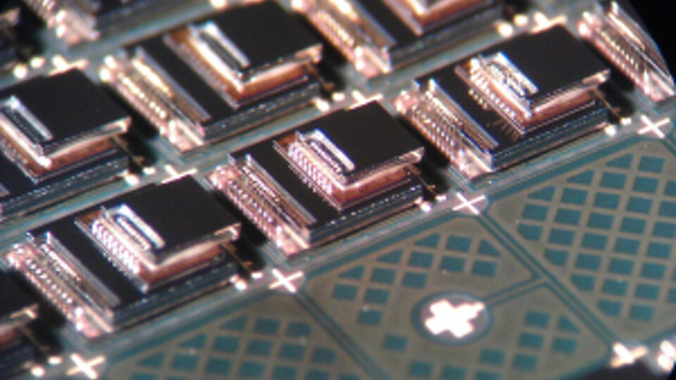
The move from lab prototypes to fab-ready components requires investment not only in MEMS design but also in ecosystem infrastructure. Foundries such as TSMC and GlobalFoundries now offer MEMS-compatible process modules. That means designers can embed MEMS elements within broader SoC or SiP projects without requiring exotic equipment or isolated fabrication lines.
Packaging has also improved. MEMS components once required bulky or custom enclosures to protect fragile elements. Today, wafer-level packaging and 3D integration techniques allow MEMS to share real estate with digital logic under standard thermal and mechanical tolerances. It opens the door to mass production and supply chain reliability.
EDA tools have also caught up with this. Simulation environments now model the electromechanical behaviors of MEMS alongside electrical and thermal performance, making co-design possible and scalable. Engineers are no longer flying blind when incorporating MEMS. They can optimize performance and layout with the same precision as digital logic.
Use Cases Driving Adoption
Several application areas are pushing MEMS into the mainstream. These include:
- Consumer electronics: MEMS microphones, gyroscopes, and accelerometers are standard in smartphones and wearables. What’s changing is how tightly these components are now being integrated with signal processing and AI inference on-device.
- Optical systems: MEMS mirrors and lens actuators are used in lidar, augmented reality, and medical imaging. Their small size and high precision make them ideal for aligning optical paths in space-constrained systems.
- Industrial IoT: Environmental sensors and vibration detectors based on MEMS enable smarter factories, predictive maintenance, and safer automation systems.
- Chip-level timing: MEMS resonators offer an alternative to quartz crystals, enabling tighter integration, better shock resistance, and potentially lower cost in high-volume devices.
These are not one-off cases. They are forming a continuous thread through the roadmaps of several large semiconductor firms and drawing investment from foundries, toolmakers, and design houses alike.
MEMS Meets Quantum, Photonics, and Beyond
As engineers explore quantum computing and advanced photonics, MEMS is finding surprising new roles. In quantum systems, MEMS can aid in cryogenic alignment, optical modulation, and shielding. In photonic circuits, MEMS actuators allow tunable waveguides, programmable optics, and thermal balancing.
This expanding relevance was noted in recent panel sessions at SPIE’s lithography conference. Discussions included not only MEMS and MOEMS integration but also their potential overlap with quantum hardware and high-NA EUV tooling strategies.
Erik Hosler shares, “Last year, we included MEMS and MOEMS, and we will keep expanding to quantum to make this a place to ask questions … Lots of great things are going on, and something will emerge.”
This statement reflects a growing recognition that MEMS is no longer separate from the road map that becomes embedded in it.
The Implications for Future Systems
As MEMS becomes a standard tool in the designer toolkit, it enables a shift in how chips are imagined. Instead of being static logic engines, chips can now sense, move, adapt, and even calibrate themselves in real-time. It redefines the boundary between hardware and environment, between computation and interaction.
In edge computing, this means more autonomous sensing systems. In automotive design, it enables smarter lidar and in-cabin monitoring. Biomedical devices support adaptive, low-power implants that respond to real-world signals. These are not just hypothetical scenarios. They are the kinds of designs now moving from proof-of-concept to tape-out.
A Quiet Development Finds Its Voice
The rise of MEMS in mainstream semiconductor design marks a quiet change. It is not about a new killer app or a radical shift in transistor technology. Instead, it is about expanding what we consider possible within a chip and doing so with tools that were once sidelined to specialty labs.
By integrating MEMS into the same flows, conversations, and roadmaps that define advanced logic and memory, the industry is not only gaining new capabilities but also learning to ask better questions about what chips should be and do. Engineers are helping ensure that those questions are heard and that the answers shape the next generation of technology.